Emerging materials science has culminated in the 2D semiconductors attracting a large amount of attention, not just due to their peculiar characteristics but also towards their possible applications. Recently, amplified spontaneous emission (ASE) due to electron-hole plasma (EHP) was witnessed in these materials, giving a big push to optoelectronic technologies.
Understanding the Basics
In order to understand this achievement, one needs to understand some basic concepts:
- 2D Semiconductors: These materials, consisting of a single layer of atoms, exhibit unusual electronic and optical properties fundamentally different from the bulk properties of those materials. An example is transition metal dichalcogenides (TMDs) such as tungsten disulfide (WS₂).
- Electron-Hole Plasma (EHP): When a semiconductor is irradiated with light, electrons become energized and transfer to a higher energy state, leaving behind ‘holes’ in their original positions. On high excitation, these electrons and holes may constitute a dense plasma.
- Amplified Spontaneous Emission (ASE): The phenomenon where stimulated emission amplifies spontaneous emission of photons to give a coherent intense light output. ASE is the key to realizing laser action in materials.
The Breakthrough Observation
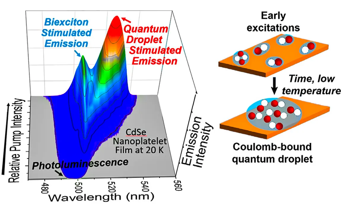
Researchers have, for the first time, witnessed ASE from EHP in 2D semiconductors. The observation was substantiated by an abrupt increase of emissions in suspended bilayer WS₂ at a certain threshold power. Such an observation attests to the switch from spontaneous to stimulated emission, a characteristic of ASE.
Significance of the Discovery
The observation is critical for the following reasons:
- Advancement in Light Sources: A realization of ASE in 2D semiconductors sets the stage to create compact, efficient, and tunable sources of light that are critical in integrated photonic circuits.
- Elucidation of Many-Body Interactions: The research informs us about complicated interactions in EHPs with reduced dimensions and deepens our basic understanding of many-body physics in 2D systems.
- Device Integration: The interfacing of 2D materials with current semiconductor technologies makes the integration of such new light-emitting devices in today’s electronic and photonic systems easy.
Challenges and Future Directions
Though this development is significant, a number of challenges still lie ahead:
- Material Quality: Achieving uniformity and minimizing defects in 2D materials are key to ASE performance consistency.
- Thermal Management: Heat management in these ultra-thin materials is essential to avoid degradation and ensure device stability.
- Scalability: Getting methods to manufacture large-area 2D semiconductors with consistent ASE properties is important for practical use.
Future research is expected to center on these issues, various 2D materials, and the incorporation of ASE-capable semiconductors in useful devices like lasers and optical amplifiers.
Broader Implications
Successful observation of ASE in 2D semiconductors has wider implications:
- Optoelectronic Devices: This application may result in more efficient LEDs, lasers, and photodetectors and contribute to advanced technologies such as high-speed communication and sensing.
- Quantum Computing: The special features of 2D materials with ASE properties could be exploited in the development of quantum information system components.
- Flexible Electronics: Since they are atomically thin, 2D semiconductors can be utilized in flexible and wearable electronic devices, leading to innovative uses in health monitoring and portable electronics.
Thus, EHP-triggered ASE in 2D semiconductors presents us with a milestone event in materials science and optoelectronics. It advances our understanding of light-matter interaction in reduced dimensions and, at the same time, opens new avenues in the development of next-generation photonic devices. The imagination of such unique applications and the transformation of various technological spheres is by no means an unrealistic assertion, given the current progress and development in research.